Silicon of the 2010s: a retrospective
The big events and trends in hardware from the past decade.
August 19, 2020
2011: Intel Sandy Bridge: the last great CPU?
The Intel Sandy Bridge family of processors was released in 2011. To understand its legacy, you have to understand the overall performance trend of CPUs the past twenty years–here’s an extremely simplified and subjective plot:
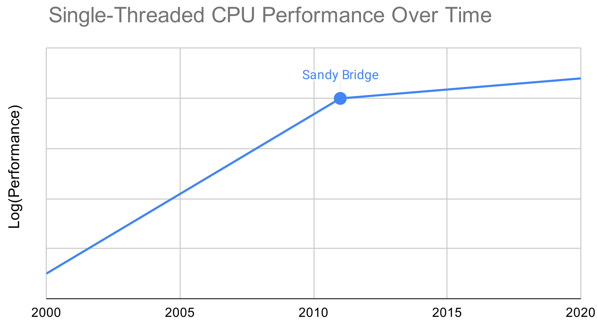
Intel’s Sandy Bridge microarchitecture was the last one to provide a serious jump in single-threaded performance. From then on, core counts have gone up, but the improvements in per-core performance have been marginal at best. Read practically any post-Sandy Bridge CPU review, and you’ll be guaranteed to find in the comment section something of the form “I’ll stick with my i5-2500K/i7-2600K/i7-2700K” (the three most well-known consumer Sandy Bridge processors). This mentality was so prevalent that Anandtech published an article in 2019 that attempted to answer, once and for all, whether it was worth upgrading a Sandy Bridge CPU, 8.5 years after its release (their conclusion was, maybe).
While I think Intel deserves some amount of criticism for their performance stagnation since Sandy Bridge, I also think it would’ve been very unrealistic for Sandy Bridge-era performance gains to have continued through today. Processor manufacturers have clearly hit the zone of diminishing returns in their efforts to translate extra transistors (from improvements in fabrication technology) to increased performance. They keep increasing cache size, branch predictor power, ROB size, etc. but a big part of their challenge is extracting more parallelism from a serial instruction stream, which has its fundamental limits. While I have no doubts CPU performance will continue to increase, I wonder if we’ll ever again see as big of a performance jump as we did in Sandy Bridge.
2013-present: custom chips become commonplace
There were a number of high-profile custom chips released this past decade:
In 2013, Canaan Creative released the first Bitcoin mining ASIC. Since then, dedicated cryptocurrency mining hardware has become a huge industry; the biggest player, Bitmain, is valued over $10B.
In 2015, Google began using TPUs in its datacenters to accelerate neural network inference (and later training). Nowadays, it’s hard to even keep track of all the AI chip startups.
In 2018, Nvidia unveiled the GeForce 20 series of GPUs, the first consumer cards with hardware-accelerated ray-tracing support. GPUs were previously more or less huge SIMD machines and actually quite general purpose, useful beyond just graphics. Nvidia added some pretty ray-tracing specific hardware, accelerating tree traversal and ray-polygon intersections.
So in summary, it’s now a lot more common for companies to invest in making customized silicon that does fairly specialized stuff. I see two primary contributors to this trend:
- Compared to a decade ago, more businesses today derive a competitive edge from computational advantages (as opposed to, say, superior customer service or branding). Today it might be worth sinking $100M+ to mine Bitcoin faster or train/serve bigger ML models, while a decade ago there were fewer ways to capitalize on an advantage in compute.
- Moore’s Law is slowing down, so custom chips have greater longetivity. Back in 2000, if your custom chip could do something 100x faster than a commercially-available chip could, you could probably expect its advantage to decay by 10x within a few years because transistor size was shrinking so rapidly. Nowadays, the decay is slower, so whatever chip you make holds its advantage for longer and provides greater net value.
2015: HBM and innovations in packaging
AMD’s Fiji series GPUs, released in 2015, were the first consumer products to feature HBM memory. Compared to previous memory technologies, HBM features a super-fat 4096-bit bus, 64 times wider than typical memory technologies. Similar to how a highway with a ton of lanes takes up a lot of land area, a 4096-bit bus requires a lot of wires. The image below shows how this can become problematic:
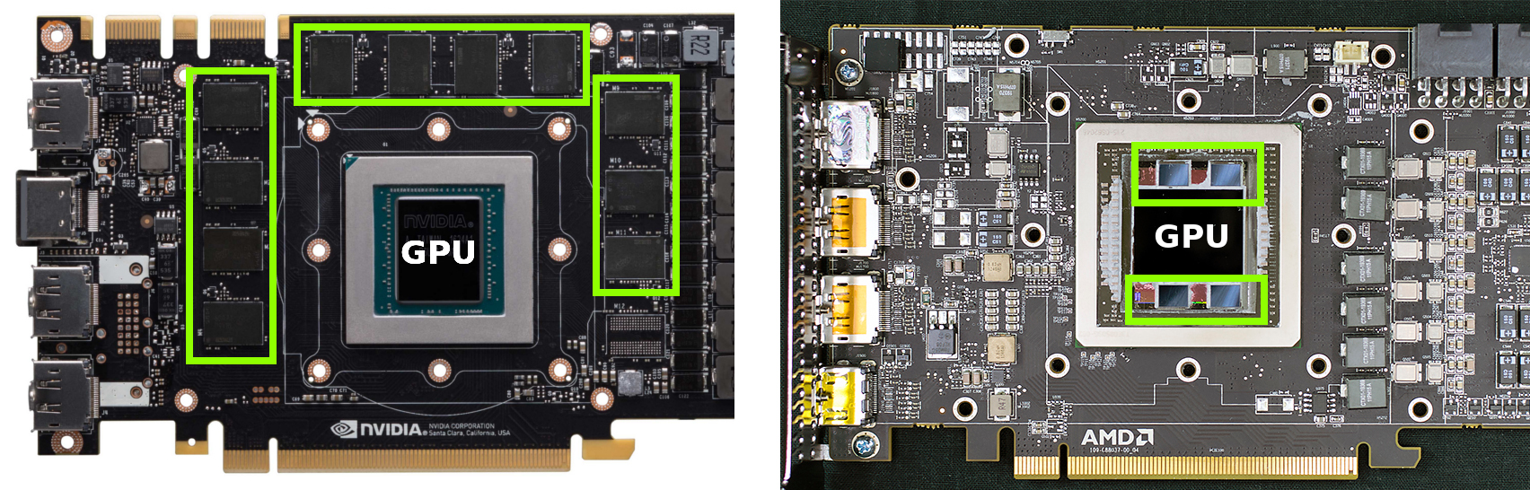
In a traditional GPU design such as the GTX 1080 Ti (above left; image source), the memory chips, demarcated in green, are totally separate from the GPU die (labeled in text). They’re connected via traces, essentially small copper wires, on the PCB. PCBs can’t handle the huge number of traces needed to support a 4096-bit bus, however, so a different approach had to be taken for Fiji.
The solution (and the same one used by every HBM-enabled GPU since) was to package the HBM memory with the GPU die. As you can see in the R9 Fury (image source) in the above right, the four memory chips demarcated in green are inside the shiny metal rectangle that forms the border of the chip package. They’re connected to the main GPU die by a silicon interposer, which can handle a much higher connection density than the PCB and therefore can support HBM’s 4096-bit bus. This multi-die approach complicated the manufacturing process but enabled much wider memory buses.
Multi-die packaging technolgies have also become popular for facilitating the production of huge chips. For a given die, a manufacturing defect anywhere in the die necessitates throwing out the entire thing. Due to this, large, monolithic dies are difficult to manufacture, which is where multi-die packaging comes to the rescue. Instead of trying to produce, say, a single 600mm2 die, you can produce six 100mm2 dies and piece them together after-the-fact. The difficulty of the former is analagous to flipping six heads in a row, while the latter is like flipping six heads total, with any number of tails in between. Naturally, this improved manufacturing yield doesn’t come for free and you pay in the form of poorer connectivity between dies–in CPUs, this generally manifests itself as slow cache coherency among cores from different dies. Still, it seems like chip makers have decided this is a worthy compromise for many designs.
Examples of multi-die technology used to improve yield for large designs include: high-end Xilinx FPGAs since 2011; AMD CPUs since 2017 (Zen, also mentioned below); a few recent, ultra-niche Intel CPUs; and a lot more Intel CPUs in the future (Intel Xeon Platinum 9200 and Project Foveros, respectively).
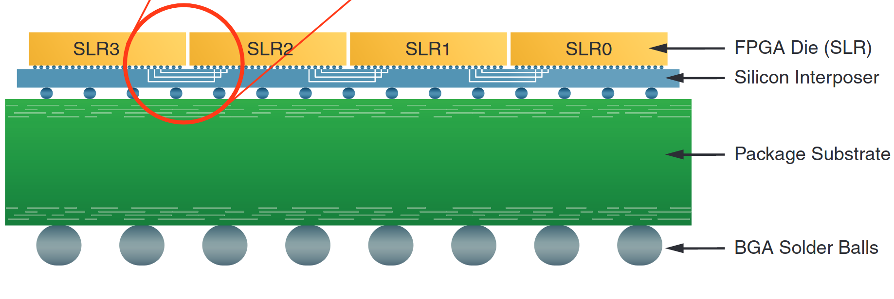
Xilinx's documentation for the Virtex-7 2000T (source) illustrates how its four dies (which Xilinx calls SLRs) are combined with an interposer. Four small FPGA dies have superior manufacturing yield than a single monolithic die.
2017: AMD Zen
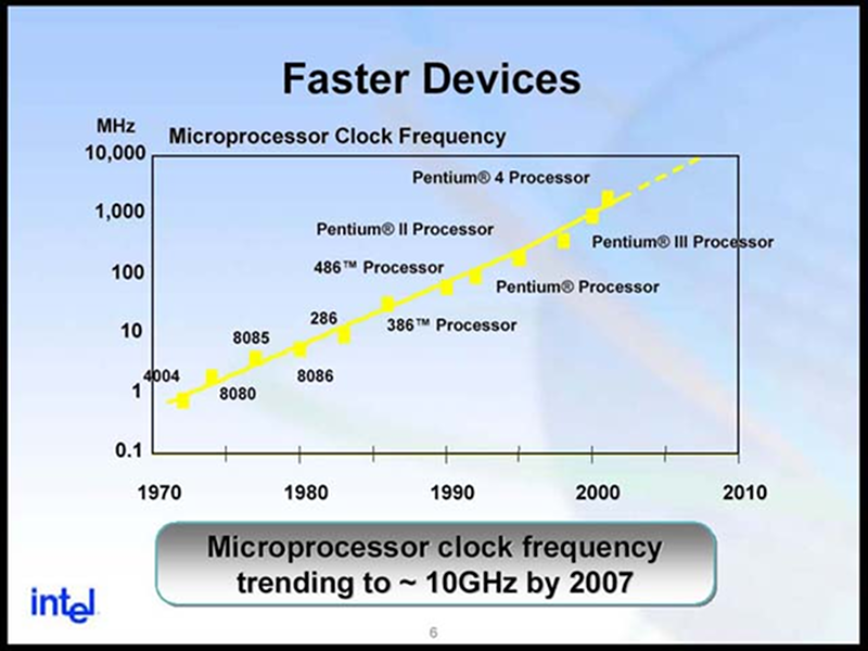
Prior to the Zen microarchitecture, AMD’s CPU division hadn’t seen happy days since 2006. That was when Intel was still hurting from its Netburst misstep–in 2000, they went all-in on clock speed and bet on NetBurst taking CPUs to 10GHz by the mid 2000s. This evidently didn’t happen (it’s 2020 and we’re at ~5GHz now) and Intel was left with ~5 years of hot and slow processors (CPU design, especially with a complete microarchitectural makeover, takes a really long time; if you make a mistake you’re stuck with it for a while). AMD released the Athlon 64 in 2004 and won the performance crown.
Young dumb & broooooke (source)
Then from 2006 to 2011, Intel delivered, back-to-back-to-back, microarchitecturally and fabrication-wise: Core to Nehalem to Sandy Bridge, 65nm to 45nm to 32nm. In the mean time, AMD released a bunch of mediocre product, and 11 years of Intel dominance ensued. For several years AMD didn’t even make high-end desktop or server CPUs–they didn’t even try to compete!
Zen was exciting because it brought AMD back into the fight–the underdog had returned, and for the first time in a very long time, the x86 processor space had serious competition. AMD’s subsequent releases have also been solid and people love to buy AMD stock.
2017: Apple A11 and the rise of Arm
The processors Apple designed in-house for their iPhones were always well-regarded, but the A11 inside the iPhone 8 / iPhone X was the chip that really started making waves. Reviewers found that no phone CPU could come close to Apple’s in performance, and in fact the A11 was competitive with Intel laptop CPUs.
I think this was a watershed moment for programmers’ perception of Arm. Arm CPUs (like the A11 and practically all mobile CPUs) were no longer just the cheap or max-power-efficiency option; they were serious competitors to x86. Since 2017 Arm has really blossomed:
- The Apple A12 (iPhone Xr, Xs, Xs Max) and A13 (iPhone 11 series) continued to push performance to incredible new levels.
- In April of 2018, a Bloomberg report was published suggesting that Apple would begin putting its own Arm processors into Macs beginning in 2020. This turned out to be true.
- Late 2018, at the AWS re:Invent conference, Amazon announced they were adding Arm-based CPU options to AWS. As a result, Arm processors are now available on the world’s largest cloud compute provider. Their offering was well-received by Anandtech.
I think the “all high-performance processors must be x86” myth persisted for so long because people mistakenly attributed x86 processor performance to intrinsic properties of the x86 instruction set architecture (ISA). In reality, if the CPU ISA is reasonable, it’s probably not holding the CPU back; what really matters is money and engineering hours invested. For a long time, Intel dominated in those two metrics, and they basically only made x86 processors, so the world was stuck with x86. Recently, however, other multi-hundred-billion dollar companies (Apple, Amazon) decided to get in the game. They couldn’t make x86-based CPUs because of patent issues (Intel and AMD are more or less the only companies that can), so they went with Arm. Lo and behold, many years and dollars spent later, we now have competitive Arm options.
2018: Spectre and Meltdown; CPU side-channel attacks
Spectre and Meltdown are perhaps the most severe hardware security vulernabilities ever disclosed to the public (who knows what the NSA is hiding). Since their disclosure in 2018, they’ve spawned an entire class of exploits, now referred to as speculative execution vulnerabilities. The Meltdown family of exploits can more or less be summarized as “we could’ve inserted this security check at this point in the CPU basically for free but didn’t, oops”; it’s the more severe bug but also the one that’s much easier to fix on future CPUs.
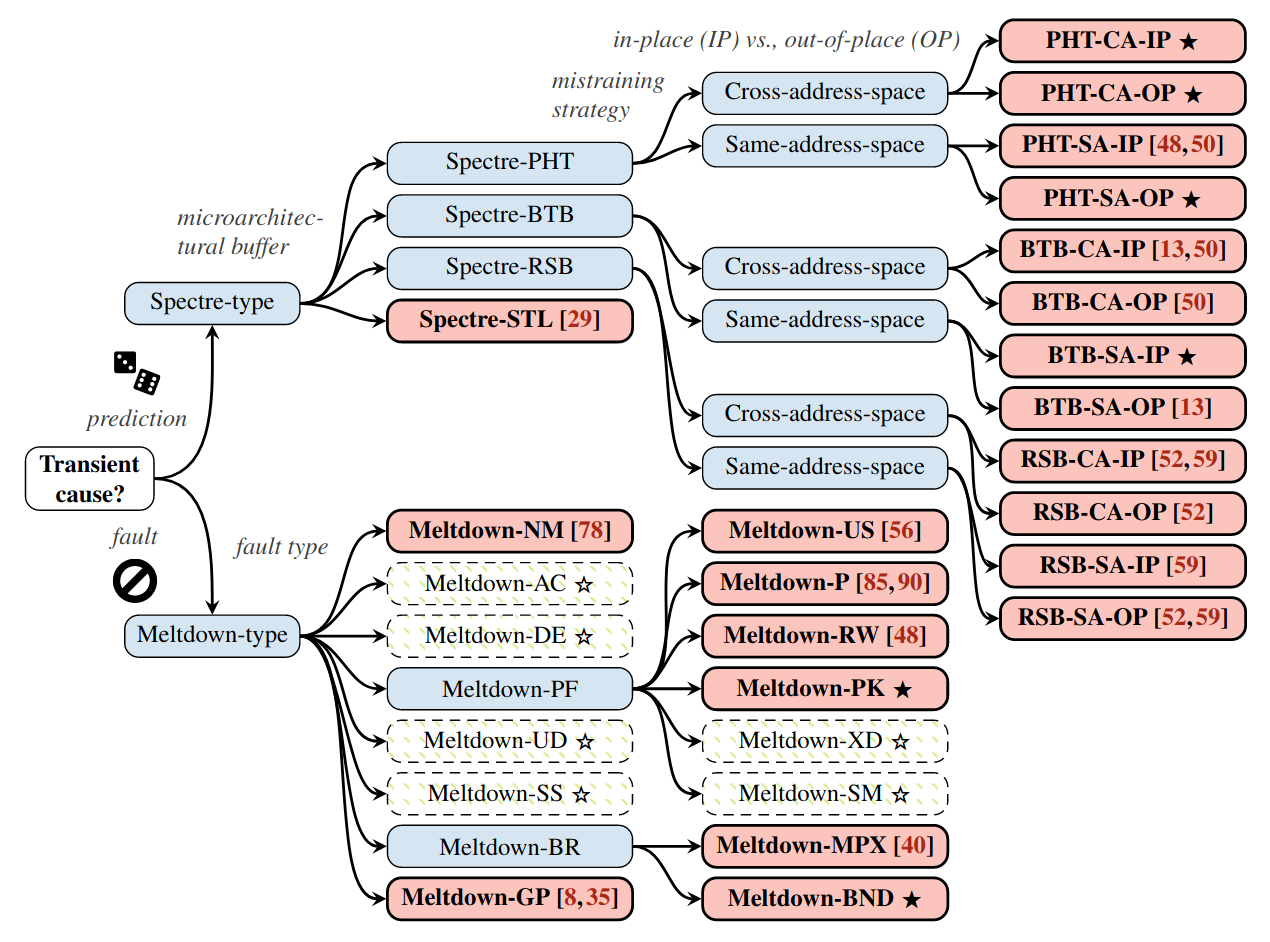
A (now outdated and incomplete) Meltdown and Spectre family tree (source)
Spectre, though, has much more ominous implications: a fundamental tradeoff between security and performance. Unlike Meltdown, Spectre isn’t so much a bug as it is a natural consequence of speculative execution. Basically, CPUs will speculatively execute the code they predict will come up next, and roll back the effects of the speculatively executed code if they guess wrong. In between the speculative execution and the rollback, though, exploits can extract information they were never allowed to access. The problem is that if an exploit can’t extract any secret information, then a normal program probably can’t extract any normal information either. In other words, the speculative execution hasn’t done anything, and you’ve essentially disabled speculative execution and made your CPU way slower. On the other hand, asking for the roll-back to occur sooner, to narrow or remove the exploitable time gap, is equivalent to just wishing for faster CPUs. They’re already doing things as fast as they can, and the whole point of speculative execution is they don’t know what code/addresses/etc. will come up in the future, so they have to guess.
It will be interesting to see how hardware and software engineers work together to mitigate Spectre. On one hand, Spectre, especially the more dangerous variants, is relatively hard to exploit, and speculative execution is hugely important for CPU performance–it basically cuts the cost of typical CPU branches (so every loop iteration and if statement) from over a dozen cycles to just a few. On the other hand, accepting a knowingly vulnerable design on the premise that its flaws are too difficult to practically exploit also seems a bit silly. Hopefully in the coming years we’ll have advanced from the current random slapdash patches to a more thorough and theoretically-grounded defense.